- 您现在的位置:买卖IC网 > Sheet目录335 > ISL97691IRTZ-TK (Intersil)IC LED DRVR BACKLIGHT 3D 16TQFN
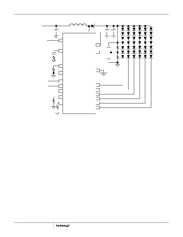
ISL97691
V BATT : 2.4V~21.8V
L1
10μH
D1
4.7μF 4.7μF
V OUT : 24.5V, 6 x 20mA
4.7μF
2.4V~5.5V
VIN
LX
100pF
470k Ω
15nF
12k Ω
COMP
ISL97691
OVP
2.2nF
23.7k Ω
ISET
53k Ω
AGND
SDA/PWMI
PGND
SCL
EN
CH1
CH2
CH3
291k Ω
FPWM
CH4
143k Ω
FSW
CH5
CH6
FIGURE 21. LED DRIVER OPERATION WITH INPUT VOLTAGE UP TO 26V
Component Selection
Circuit” on page 1, sets V OVP (typ) to 25.41V (Equation 6).
V OVP ( typ ) = 1.22V × ---------------------------- = 25.41V
The design of the boost converter is simplified by an internal
compensation scheme allowing easy design without complicated
470 + 23.7
23.7
(EQ. 6)
calculations. Please select your component values using the
recommendations below.
The OVP threshold, R 1 , and R 2 tolerances should also be taken
into account (Equations 7 and 8).
V OVP ( min ) = 1.18V × ----------------------------------------------
V OVP ( max ) = 1.24V × ----------------------------------------------
Input Capacitor
It is recommended that a 4.7μF to 10μF X5R/X7R or equivalent
ceramic input capacitor is used.
Overvoltage Protection (OVP)
R1min + R2max
R2max
R1max + R2min
R2min
(EQ. 7)
(EQ. 8)
The integrated OVP circuit monitors the boost output voltage, V OUT ,
and keeps the voltage at a safe level. The OVP threshold is set as
shown in Equation 5:
Calculating V OVP using the OVP threshold range (1.18V to 1.24V)
and 0.1% resistor tolerances gives an actual V OVP range of 24.53V
to 25.88V for the 25.4V example above (Equations 9 and 10).
V OVP ( typ ) = 1.22V × ----------------------
V OVP ( min ) = 1.18V × -------------------------------------------------------------------------------- = 24.53V
( 23.7 × 1.001 )
Where:
R1 + R2
R2
(EQ. 5)
( 470 × 0.999 ) + ( 23.7 × 1.001 )
(EQ. 9)
V OVP ( max ) = 1.24V × -------------------------------------------------------------------------------- = 25.88V
V OVP is the maximum boost output voltage, V OUT (V)
R 1 is the resistor from OVP pin to the boost output ( ? )
R 2 is the resistor from OVP pin to GND ( ? )
The total R 1 plus R 2 series resistance should be high to minimize
power loss through the resistor network. For example, choosing
R 1 = 470k ? and R 2 = 23.7k ? per the “Typical Application
13
( 470 × 1.001 ) + ( 23.7 × 0.999 )
( 23.7 × 0.999 )
(EQ. 10)
It is recommended that parallel capacitors are placed across the
OVP resistors such that R 1 /R 2 = C 2 /C 1 . Using a C 1 value of at
least 30pF is recommended. These capacitors reduce the AC
impedance of the OVP node, which reduces noise susceptibility
when using high value resistors.
FN7840.1
February 1, 2013
发布紧急采购,3分钟左右您将得到回复。
相关PDF资料
ISL97693IRTZ-TK
IC LED DRVR BACKLIGHT 16TQFN
ISL97901CRZ
IC LED DRVR 1.5A 28QFN
ISO1I811T
ISOLAT DGTL 500VAC 8CH 48TSSOP
ISO7221AQDRQ1
IC DGTL ISOLATOR 1MBPS DL 8SOIC
ISOBAR4 ULTRA
SURGE SUPPRSSR 4OUT 6'CORD W/LED
ISOBAR6 ULTRA
SURGE SUPPRSSR 6OUT 6'CORD W/LED
ISOBAR6DBS
SURGE SUPP DSS 6OUT 6'CORD W/LED
ISOBAR6ULTRAHG
SURGE SUPP 6OUT 15'CORD HOSP GRD
相关代理商/技术参数
ISL97692IIZ-T
制造商:Intersil Corporation 功能描述:4 CH W/12-BIT PWM DIMMING SINGLE CELL LI-ION BATTERY POWERED - Tape and Reel
ISL97692IRTZ
制造商:Intersil Corporation 功能描述:4 CH W/12-BIT PWM DIMMING SINGLE CELL LI-ION BATTERY POWERED - Rail/Tube 制造商:Intersil Corporation 功能描述:IC LED DRVR BACKLIGHT 16TQFN 制造商:Intersil 功能描述:4CH w/12Bit PWM Dim Li-ION LED Driver
ISL97692IRTZ-T
制造商:Intersil Corporation 功能描述:4 CH W/12-BIT PWM DIMMING SINGLE CELL LI-ION BATTERY POWERED - Tape and Reel 制造商:Intersil 功能描述:4CH w/12Bit Dimming Li-Ion LED Driver
ISL97692IRTZ-TK
制造商:Intersil Corporation 功能描述:4 CH W/12-BIT PWM DIMMING SINGLE CELL LI-ION BATTERY POWERED - Tape and Reel 制造商:Intersil Corporation 功能描述:IC LED DRVR BACKLIGHT 16TQFN 制造商:Intersil 功能描述:4CH w/12Bit Dimming Li-Ion LED Driver
ISL97693IRTZ
功能描述:IC LED DRVR BACKLIGHT 16TQFN RoHS:是 类别:集成电路 (IC) >> PMIC - LED 驱动器 系列:- 产品培训模块:Lead (SnPb) Finish for COTS
Obsolescence Mitigation Program 标准包装:2,500 系列:- 恒定电流:- 恒定电压:- 拓扑:升压(升压),切换式电容器(充电泵) 输出数:1 内部驱动器:是 类型 - 主要:背光 类型 - 次要:白色 LED 频率:625kHz ~ 875kHz 电源电压:2.7 V ~ 5.3 V 输出电压:5V 安装类型:表面贴装 封装/外壳:10-TFSOP,10-MSOP(0.118",3.00mm 宽) 供应商设备封装:10-µMAX 包装:带卷 (TR) 工作温度:-40°C ~ 85°C
ISL97693IRTZ-T
功能描述:IC LED DRVR BACKLIGHT 16TQFN RoHS:是 类别:集成电路 (IC) >> PMIC - LED 驱动器 系列:- 产品培训模块:Lead (SnPb) Finish for COTS
Obsolescence Mitigation Program 标准包装:2,500 系列:- 恒定电流:- 恒定电压:- 拓扑:升压(升压),切换式电容器(充电泵) 输出数:1 内部驱动器:是 类型 - 主要:背光 类型 - 次要:白色 LED 频率:625kHz ~ 875kHz 电源电压:2.7 V ~ 5.3 V 输出电压:5V 安装类型:表面贴装 封装/外壳:10-TFSOP,10-MSOP(0.118",3.00mm 宽) 供应商设备封装:10-µMAX 包装:带卷 (TR) 工作温度:-40°C ~ 85°C
ISL97693IRTZ-TK
功能描述:IC LED DRVR BACKLIGHT 16TQFN RoHS:是 类别:集成电路 (IC) >> PMIC - LED 驱动器 系列:- 产品培训模块:Lead (SnPb) Finish for COTS
Obsolescence Mitigation Program 标准包装:2,500 系列:- 恒定电流:- 恒定电压:- 拓扑:升压(升压),切换式电容器(充电泵) 输出数:1 内部驱动器:是 类型 - 主要:背光 类型 - 次要:白色 LED 频率:625kHz ~ 875kHz 电源电压:2.7 V ~ 5.3 V 输出电压:5V 安装类型:表面贴装 封装/外壳:10-TFSOP,10-MSOP(0.118",3.00mm 宽) 供应商设备封装:10-µMAX 包装:带卷 (TR) 工作温度:-40°C ~ 85°C
ISL97694AIRTZ
制造商:Intersil Corporation 功能描述:6 CH W/12-BIT PWM DIMMING SINGLE CELL LI-ION BATTERY POWERED - Rail/Tube 制造商:Intersil Corporation 功能描述:IC LED DRVR BACKLIGHT 20TQFN
